Antiferroelectric substances possess electrical characteristics that are beneficial for utilization in high-capacity energy storage solutions. However, scientists have recently uncovered that there is a specific size limit beyond which these materials lose their advantageous electrical properties and become ferroelectric.
As electronic devices continue to shrink in size, it is becoming increasingly crucial to comprehend how a material's properties can alter when reduced to small scales, says Ruijuan Xu, an assistant professor of materials science and engineering at North Carolina State University and the corresponding author of a related research paper.
Thin Antiferroelectric Materials
The research studied antiferroelectric materials, which have a crystalline structure composed of repeating units that possess a positive and negative charge, referred to as a "dipole." These dipoles alternate throughout the structure, making antiferroelectrics unique. However, the research found that when antiferroelectric thin films become too thin, they experience a phase transition and transform into ferroelectric materials, hindering their effectiveness for energy storage. On the other hand, this transition presents new opportunities for memory storage applications.
In simpler terms, antiferroelectric materials have regularly spaced positive and negative charges, so that one unit has the positive charge on top and the negative charge on the bottom, while the next unit has the positive charge on the bottom and the negative charge on top. This arrangement results in no net polarization at the macro level. Ferroelectrics, on the other hand, have a crystalline structure where all the repeating units have their dipoles pointing in the same direction. The polarization in ferroelectrics can be reversed by an applied electric field. The researchers looked into lead-free sodium niobate (NaNbO3) membranes to investigate how the properties of antiferroelectrics change at small scales.
The scientists added a sacrificial buffer layer between the antiferroelectric thin film and the substrate to address this problem, according to Xu. Once the thin film had reached the desired thickness, they carefully etched the sacrificial layer. The team was able to separate the thin film from the substrate as a result of this. Finally, knowing that the substrate was not causing any changes allowed us to determine how any changes in the thin film are affected by its size.

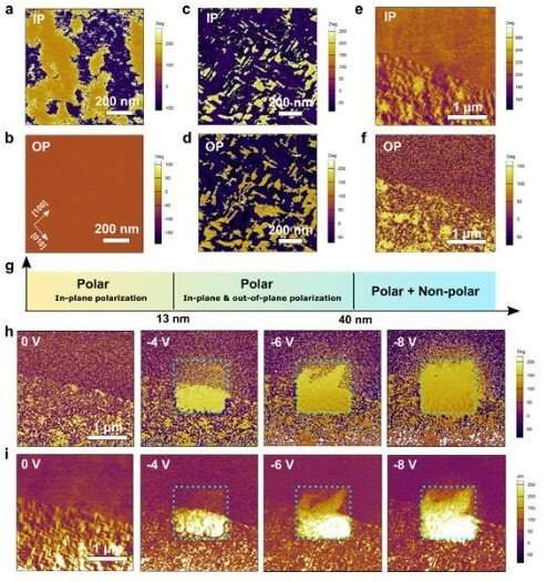
Piezoresponse force microscopy (PFM) of emergent ferroelectricity and phase coexistence in NaNbO3 membranes. Lateral and vertical PFM phase images obtained for a) and b) 13 nm, c) and d) 40 nm, and e) and f) 100 nm thick membranes, respectively. g)
ALSO READ: New Study Might Explain Crystalline Ice's Anomalous Behavior
Structural Distortion on Membrane's Surface
The team was able to deduce from the first principles that the structural distortion that originates on the membrane's surface is what causes the phase changes they observe in extremely thin antiferroelectric materials. The researchers then used a variety of experimental and theoretical techniques to evaluate these strain-free samples at thicknesses ranging from 9 nanometers (nm) to 164 nm. Xu claimed that the results were quite unexpected.
The group also stated that they are aware that alternating dipoles are present at the atomic level in antiferroelectric materials like lead-free NaNbO3 membranes. At a thickness of under 40 nm, they found that the NaNbO3 membranes completely transition to ferroelectricity. They added that the material had some ferroelectric and some antiferroelectric regions between 40 nm and 164 nm. Based on their experimental findings, the researchers extrapolated that any thickness of NaNbO3 below 270 nm would have at least a few ferroelectric regions, according to a report in Phys.
Xu stated that they have given important insights into how they can control a material's properties by utilizing size effects, but he doesn't want to speculate too much about potential applications at that time. The methods they employed to identify those effects can be applied to answer related queries for a variety of other materials. In NaNbO3, the researchers have found important size effects.
RELATED ARTICLE: Storage technology Discovered For Continuous Fluctuating Renewable Energy, High Power Performance With Density Factor
Check out more news and information on Antiferroelectric Materials in Science Times.


