Controlled charge flows are vital to many science fields since they carry energy and information. They serve as probes of material properties and dynamics and are also used in revealing and inducing broken symmetries.

Generating Fast and Adaptable Current
Conventional microelectronics architectures, composed of transistors to control electrical currents along wires, power many devices, from advanced computers to simple gadgets. However, integrated circuits offer diminishing returns in terms of speed and adaptability.
Emerging technologies for light-based current control provide promising routes beyond the limitations of conventional systems. However, experts still face the challenge of maintaining optical generation and manipulating currents at nanometer spatial scales. This has been a vital step towards scalable optoelectronic systems for microelectronics and information science.
Potential of Light-Driven Electric Current
At Los Alamos National Laboratory, researchers developed nanometer-scale light-based systems. Their innovation can deliver breakthroughs in various technological applications, such as room-temperature infrared detection and ultrafast microelectronics. The result of their experiment is discussed in the paper "Light-driven nanoscale vectorial currents."
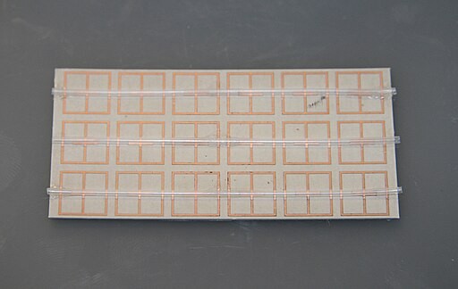
In this study, the research team designed and constructed asymmetric, nano-sized gold structures on a thin layer of graphene. These structures are known as "nanoantennas" since the way they capture and focus light waves allows them to form optical "hot spots" that excite electrons. In this system, only the graphene electrons near the hot spots are excited, while the remaining graphene remains less excited.
As the experts adopted a teardrop shape of gold nanoantennas, breaking inversion symmetry defines a directionality along the structure. Meanwhile, the hot spots at the sharp tips of the nanoantennas lead to a pathway where the excited hot electrons flow with net directionality.
The resulting charge current was controllable and tunable at the nanometer scale by exciting various combinations of hot spots. According to research supervisor Hou-Tong Chen, metasurfaces offer an easy way of controlling the location, amplitude, and direction of hot spots and nanoscale charge currents with a faster response speed than a picosecond.
The development of optoelectronic metasurfaces has lots of promising applications. Since the generated charge current can be utilized as the signal for photodetection, it can be harnessed for long-wavelength infrared regions.
Additionally, the system can be a source of terahertz radiation, which can be used in various applications, from ultra-high-speed wireless communications to spectroscopy characterization of materials. It can also provide new opportunities for controlling nanomagnetism, where the specialized currents can be designed for adaptable, nanoscale magnetic fields.
The new capability exhibited by the metasurface can play an important role in ultrafast information processing, such as microelectronics and computing. Since the new system enables laser pulses and metasurfaces for adaptive circuits, slower and less versatile transistor-based computer and electronic architectures can be dispatched.
The result of the study lays the groundwork for versatile patterning and optical control over nanoscale electric currents. Compared to conventional circuits, the adaptive structured light fields can provide completely new design options.
RELATED ARTICLE: New 2D Bilayer Innovation Expected to Improve Electronic and Optoelectronic Devices
Check out more news and information on Optoelectronics in Science Times.


