New research conducted by an international team developed a new tool that could serve as the transistor of the future. This tiny device was created through the help of an electron microscope, allowing experts to develop a transistor that scales 25,000 smaller than the strand of human hair.
The research was made possible through the help of experts from various fields, which dedicated their efforts straight from Russia, Japan, Australia, and China. The study presented had a series of examinations carried on for the past five years. This year, their comprehensive product was revealed to the public, which may offer the key to the untapped capacity of electronics and communication technology.
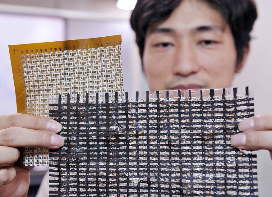
Tiniest Transistor Made from Carbon Nanotube
Queensland University of Technology (QUT) and National Institute for Materials Science (NIMS) expert Dmitri Golberg, who led the recent paper, said in a California News Times report that the results their team found had met the fundamental discovery were interested in uncovering. According to the expert, the innovation found in the study will pave the way for future developments of transistors and other devices related to modern-day computing functions.
Golberg explained that their work is a testament to the current knowledge on electronics to manipulate and modify properties found in a carbon nanotube. Throughout the study, the authors were able to heat up layers of carbon nanotubes until the lone, inner layer of the tube remained. The process was done through an application of force simultaneously backed up by low voltage, which produced the tiny transistors.
Behind the scenes, the chirality of the nanotube changed by heat and constant strain. This led the carbon atoms to form bonds, resulting in a single-atomic layer formation. Basically, these complex steps allowed the composition of the nanotube walls to rearrange into microscopic transistors.
Nanotube Transistor Key to Fabricating Nanoscale Electronic Devices
The theory regarding the changes of the atomic structures and other compositions in the transistor was observed and detailed with the expertise of the collaborative team from the National University of Science and Technology in Moscow.
NIMS International Center for Materials Nanoarchitectonics (MANA) expert and lead author of the study Dai-Ming Tang said in a SciTechDaily report that the recent examinations on the tiny transistors show potential manipulation and full control of the nanotube's molecular characteristics on fabricating electrical devices that are measured on a nanoscale level.
Tang has been on the project's development for over five years now. The study was most;y conducted with the assistance of Golberg and other research colleagues at the same laboratory center. Tang said that the ability of the carbon nanotubes to conduct electricity shared a glimpse of energy-efficient nano transistors, a technology far greater than silicon-based microprocessors available in today's time.
The paper's follow-up investigations will include several analyses on the chirality of each of the carbon nanotubes, its geometry, and electronic capacity. The coverage was published in the journal Science, titled "Semiconductor nanochannels in metallic carbon nanotubes by thermomechanical chirality alteration."
RELATED ARTICLE : Nanotech in Medical Imaging, Security Screening; Researchers Reveal How Nanocomposite Works for 'Picture-Perfect' X-ray Scans
Check out more news and information on Nanotechnology in Science Times.
© 2026 ScienceTimes.com All rights reserved. Do not reproduce without permission. The window to the world of Science Times.


